INTRODUCTION
Flip flops are the basic timed memory elements in electronics.As timing is an important factor in precise and useful circuit building, flip flops serve in an inevitable role.The main difference between latch and a flip flop is that , flip flop has a clock , which is used to provide time reference for its action.Flip flops are available in the form of integrated circuit packages , with more than two flip flops in one package.An enthusiast in electronics would be more familiar with those and we could easily use it with the help of the datasheet provided and could possibly build different circuits.But it would be more fun to know about the detailed working of those and lets try to build a discrete version of one of the most basic flip flops - 'The T - flip flop'.


BASIC CONCEPT
T-flip flop or Toggle flip flops are simple and widely used flip flops.As the name indicates , this flip flop toggles or inverts the output for each clock cycle.That is , when the clock is triggered , the output will be flipped by this flip flop.If the output was high , then it will become low and vice versa.
T flip flops can be edge triggered or level triggered.
In a level triggered flip flop the output will be toggled as long as the clock is in the triggering level.
In an edge triggered flip flop , the output will be toggled only at the trigger-edge occurrence time.There is both positive and negative edge triggered circuits.
A positive edge triggered T flip flop has a timing diagram as shown below :

As it is clear from the above timing diagram, When the positive edge of the clock is engaged , then the output will toggle its present value and it will sustain its output until the next triggering encounters.
So, by close observation , one could identify its important application in practical circuits.
Yes, it is used as a frequency divider circuit in circuit.That is ,when the clock signal has completed 2 cycles , then the output has completed only 1 cycle. Which means, this circuit can be used as a frequency divide by 2 circuit.Thus by coupling 'n' toggle flip flops , we could build a '2^n' frequency divide circuit.
TRUTH TABLE
Usually the toggle flip flops have an enable pin , either high enable or low enable.This pin determines the normal working of the flip flop.If this pin is hold inactive , then the flip flop will not respond to the clock cycles.In advance to that some packages also have a preset and clear pins , which is used to pre-define the initial output values of the flip flop.
The simple truth table is shown below :

CIRCUIT AND CONSTRUCTION
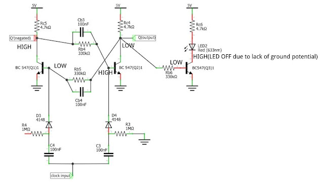
The circuit for building a T flip flop is shown below. The circuit is a positive edge triggered circuit(which is described through), and is quite easy to build.

The circuit has mainly three sections.They are :
1. The differentiator section
2. The Latch section
3. The output section

Each sections are explained one by one below.
1.THE DIFFERENTIATOR SECTION
Differentiator circuit is basically a high pass filter.Here the differentiator is used to make the circuit an edge triggered circuit.The differentiator , as shown in the below diagram, is used to transform the square shaped wave from the clock input into positive pulses , to which the above latch circuit will respond.

For each clock trigger (positive going) , this section creates an impulse signal at the cathode terminal of both diodes D1 and D2, at the same time.The next section (latch section) will toggles the output in response to this created impulses from the differentiator section.
2.THE LATCH SECTION
The latch section is shown below :

The basic working of a latch section is explained in the previous blog.This section provide stable output , until next trigger pulse arrives.
3.THE OUTPUT SECTION

The output section includes only an LED as the load to a transistor.This transistor is synchronously switched with the output transistor Q2, and the LED will be turned ON and OFF accordingly , just to make the output more observable.
CIRCUIT WORKING
Observing the circuit ,it is clear that the transistors Q1 and Q2, along with its biasing resistors forms the latching part.
**(Latch circuit using transistors is described in an early blog.The link is provided at the end.)**
This combination will hold the output steady , until the next clock pulse arrives.As an additional component , two capacitors are provided parallel to the base resistors, in the latch part.This is to ensure adequate switching speed with the clock pulses.
Consider , initially transistor Q1 is OFF and Q2 is ON.Which means , the base of the transistor Q2 is HIGH (1) and the base of the transistor Q1 is LOW(0).
Then the collector of the transistor Q2 is having LOW , as the transistor switches the ground potential to the collector of the transistor Q2.
So output is LOW.
Indicating the LOW potential , the LED will be OFF because the potential at the base of the transistor driving the LED is connected to the collector of the transistor Q2 , which is now at the LOW state.
The situation is depicted in the below figure :

Consider the above situation as the power ON situation.
After the clock pulses are enabled , the situation changes accordingly.
Now,the base of Q1 is LOW and that of Q2 is HIGH.
Let a clock signal be applied as depicted in the below figure. Then the differentiator circuit will provide an impulse signal at the cathode terminal of both the diodes provide.
The impulse signal will reaches the base of both the transistors Q1 and Q2.
Q2 is already in the HIGH state ,so the high pulse is irrelevant for it.
Q1 ,which is at the LOW state ,is triggered by this positive impulse.The base of Q1 receives an instantaneous high pulse which will immediately switches its collector to the ground potential.
This ground potential is instantaneously coupled to the base of the transistor Q2 ,through the instant response of the parallel switching capacitor to its base.
This forces the Q2 to its OFF state and Q1 to its ON state transition , instantaneously.
This transition is stabilized by the biasing resistors and will stably sustain the changed outputs ,till the next clock pulse arrive.
observe the following depiction :

Q2 pulled to OFF state means the collector of Q2 is having HIGH potential , which is coupled to the base of the LED indicator driving transistor.
This forces the driving transistor to be at the ON state and as a result the cathode of the indicator LED acquires ground potential , which lite it up , indicating the HIGH output state.
Thus in short , Initially, the output terminal (Q) was at the LOW state, at power ON.
Then,as the clock pulse arrived , the output flips to HIGH state ,in response to the clock.
This circuit is working as a T-flip flop i.e., flipping the output with each clock pulses.
Thus with each clock pulse, the output will toggle.
So , ironically, for one complete clock pulse there is a half completed output cycle or in other way, we could get a complete output cycle only after two complete clock pulses.
Thus the circuit acts as a frequency divider,more clearly a 'frequency divide by two' circuit.
The timing diagram shown in the beginning explains this concept clearly.
To add up a little fun,lets do one more thing.
To force the output of Q1 as LOW initially, we could add a 'power ON reset' circuit.So that each time when we power up the ciruit , the output will initially be zero, by forcing the base of Q2 to HIGH state.
Power on reset can be done by incorporating the following circuit :

The collector terminal of the above circuit is capable of providing an instantaneous LOW state ,and when this terminal is coupled to the base of Q1 transistor, it will be driven to its OFF state , which forces the Q2 to its ON state in turn , and thus the output terminal will be LOW when the power is ON.
The final connected circuit is shown below :

Thus, we successfully tried out to build a toggle flip flop using transistors.Its always fun to play with basic components.Next we could try to build a D-flip flop.
Feel free to read the explanation of latch circuit using the following link :
Thank you!!!!!!!
your blog is so good pls make d flip flop pls
ReplyDelete