INTRODUCTION
A latch circuit is basically a memory circuit.It will holds the output which is given as the input,as long as power is supplied.It is a basic volatile memory which we could easily build.Latch is a brilliant use of two inverter circuits and it works perfectly.A latch circuit can be used to make different flip flop circuits which we could do in the future discussions.So without further delay we could build a latch circuit.
WORKING PRINCIPLE
Transistor inverter circuits coupled together will make a latch circuit.Now just observe the following circuit configuration.


The following circuit demonstrates the above configuration :

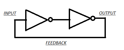
In the above circuit , the orange line is the feed back line and when we apply the input for a short instance , then this will propagate through the transistors and outputs it.This is fed back and the circuit latches the same.The digital logic representation is as below :
PRACTICAL IMPLEMENTATION
We could just wire up the circuit in the bread board and just observe the output by giving an indicator LED with a driver circuit.The circuit is as below :

The PS1 and PS2 are the two push switches, whose one side terminals are connected to logic high and logic low respectively.The other terminal of the two push switches are shorted and connected to the input terminal of our latch circuit.When we press the PS1 , a 5 volt is applied at the input at that instant and the circuit latches it.When we press PS2 , then zero volt is applied at the input and the circuit latches it.The latch can be visualized by the ON and OFF states of the LED.The LED is ON when the latched output is high.The LED is OFF when the latch output is low.A capacitor (preferably 0.1 micro farad) is advised to be connected parallel with the switches to ensure effective error free switching.

The PS1 and PS2 are the two push switches, whose one side terminals are connected to logic high and logic low respectively.The other terminal of the two push switches are shorted and connected to the input terminal of our latch circuit.When we press the PS1 , a 5 volt is applied at the input at that instant and the circuit latches it.When we press PS2 , then zero volt is applied at the input and the circuit latches it.The latch can be visualized by the ON and OFF states of the LED.The LED is ON when the latched output is high.The LED is OFF when the latch output is low.A capacitor (preferably 0.1 micro farad) is advised to be connected parallel with the switches to ensure effective error free switching.
PRACTICAL OBSERVATION
When implemented , the circuit works just fine.It is drawing about 4.1 milli ampere current when the output is low and is drawing about 4.5 milli ampere current when the output is high.The implemented circuit is shown in the following figures.
1. The wired circuit when the input is HIGH :

2. The wired circuit when the output is LOW :

By changing the resistors of the base and the collector we could adjust the base and collector currents and adjust the power conception of the circuit which will be useful in doing coupled circuit with more number of latches.
We could add an additional feature to the circuit just for fun.We could add an enable pin to the latch circuit.The configuration is shown in the following figure :
 Here , the enable pin will just control the entire latch circuit.If we make the enable pin low , the operation of the latch is in normal condition.If the enable pin is high , then the input pin is kept low all the time and this will hold the output as low , irrespective of the input provided by the push switches.Thus we could develop different modification to our circuit to meet our needs and thus can have much more fun.
That's all for this discussion.Hope you had some fun and knowledge..
If you are not familiar with the transistor inverter circuit explained here feel free to visit this article :
https://electrojubilance.blogspot.com/2019/03/not-gate-inverter-logic-using.html
Thank you...!!!
1. The wired circuit when the input is HIGH :


By changing the resistors of the base and the collector we could adjust the base and collector currents and adjust the power conception of the circuit which will be useful in doing coupled circuit with more number of latches.
We could add an additional feature to the circuit just for fun.We could add an enable pin to the latch circuit.The configuration is shown in the following figure :

That's all for this discussion.Hope you had some fun and knowledge..
If you are not familiar with the transistor inverter circuit explained here feel free to visit this article :
https://electrojubilance.blogspot.com/2019/03/not-gate-inverter-logic-using.html
Thank you...!!!
I like it...I do make memories for my projects but my 1 bit memory I usually make 2 capacitor n 2 transistors
ReplyDeleteflip flop then i minus one capacitor.. Wow this a different version I have learn today
Sorry, but you blew up your Power Supply & damaged switch PS1, Q1 &/or Q4 whenever you use PS1. A fundamental mistake & an example of hobbyist know it all. You're shorting +5, through switch PS1, to Gnd through the Emitter diodes of Q1/Q4. You may not notice it over a short period of time with short switching pulses but slowly it's happening. If the 2 switches are independent & pressed simultaneously you'll blow or damage your +5 supply & PS1. A small carefully chosen series resistance to PS1 could help, otherwise good job.
ReplyDeleteActually, Q4 should be ok as long as it's Base resistor is large enough.
ReplyDelete